- 您现在的位置:买卖IC网 > Sheet目录320 > DK-DEV-4SE530N (Altera)KIT DEV STRATIX IV FPGA 4SE530
�� �
�
�Chapter� 6:� Board� Test� System�
�6–5�
�Using� the� Board� Test� System�
�The� Config� Tab�
�The� Config� tab� shows� information� about� the� board’s� current� configuration.�
��MAX� II� registers,� the� JTAG� chain,� the� board’s� MAC� address,� the� flash� memory� map,�
�and� other� details� stored� on� the� board.�
�The� following� sections� describe� the� controls� on� the� Config� tab.�
�Board� Information�
�The� Board� information� controls� display� static� information� about� your� board.�
�■�
�■�
�MAX� II� ver� —Indicates� the� version� of� MAX� II� code� currently� running� on� the� board.�
�The� MAX� II� code� resides� in� the� <install�
�dir>� \kits\stratixIVE_4se530_fpga\examples� directory.� Newer� revisions� of� this�
�code� might� be� available� on� the� Stratix� IV� E� FPGA� Development� Kit� page� of� the�
�Altera� website.�
�MAC� —Indicates� the� MAC� address� of� the� board.�
�MAX� II� Registers�
�The� MAX� II� registers� control� allow� you� to� view� and� change� the� current� MAX� II�
�register� values� as� described� in� Table� 6–1� .� Changes� to� the� register� values� with� the� GUI�
�take� effect� immediately.� For� example,� writing� a� 0� to� SRST� resets� the� board.�
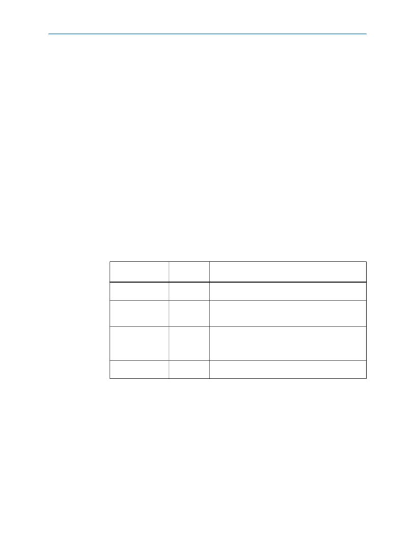
�Table� 6–1.� MAX� II� Registers�
�Register� Name�
�System� Reset�
�(SRST)�
�Page� Select� Register�
�(PSR)�
�Page� Select� Override�
�(PSO)�
�Page� Select� Switch�
�(PSS)�
�Read/Write�
�Capability�
�Write� only�
�Read� /� Write�
�Read� /� Write�
�Read� only�
�Description�
�Set� to� 0� to� initiate� an� FPGA� reconfiguration.�
�Determines� which� of� the� up� to� eight� (0-7)� pages� of� flash�
�memory� to� use� for� FPGA� reconfiguration.� The� flash� memory�
�ships� with� pages� 0� and� 1� preconfigured.�
�When� set� to� 0,� the� value� in� PSR� determines� the� page� of�
�flash� memory� to� use� for� FPGA� reconfiguration.� When� set� to�
�1,� the� value� in� PSS� determines� the� page� of� flash� memory� to�
�use� for� FPGA� reconfiguration.�
�Holds� the� current� value� of� the� rotary� switch� (SW5).�
�■�
�PSO� —Sets� the� MAX� II� PSO� register.� The� following� options� are� available:�
�■�
�■�
�Use� PSR� —Allows� the� PSR� to� determine� the� page� of� flash� memory� to� use� for�
�FPGA� reconfiguration.�
�Use� PSS� —Allows� the� PSS� to� determine� the� page� of� flash� memory� to� use� for�
�FPGA� reconfiguration.�
�■�
�■�
�PSR� —Sets� the� MAX� II� PSR� register.� The� numerical� values� in� the� list� corresponds� to�
��for� more� information.�
�PSS� —Displays� the� MAX� II� PSS� register� value.� Refer� to� Table� 6–1� for� the� list� of�
�available� options.�
�June� 2011�
�Altera� Corporation�
�Stratix� IV� E� FPGA� Development� Kit� User� Guide�
�发布紧急采购,3分钟左右您将得到回复。
相关PDF资料
DK-DEV-4SGX530N
KIT DEVELOPMENT STRATIX IV
DK-DEV-5AGXB3N/ES
ARRIA V DEVELOPMENT KIT
DK-DEV-5M570ZN
KIT DEV MAX V 5M570Z
DK-DEV-5SGXEA7N
KIT DEV STRATIX V FPGA 5SGXEA7
DK-DSP-2S180N
DSP PRO KIT W/SII EP2S180N
DK-DSP-3C120N
KIT DEV DSP CYCLONE III EDITION
DK-K7-CONN-CES-G
KINTEX-7 FPGA CONNECTIVITY KIT
DK-K7-EMBD-CES-G-J
KINTEX-7 FPGA EMBEDDED KIT JAPAN
相关代理商/技术参数
DK-DEV-4SGX230N
功能描述:可编程逻辑 IC 开发工具 FPGA Development Kit For EP4SGX230KF40C2N
RoHS:否 制造商:Altera Corporation 产品:Development Kits 类型:FPGA 工具用于评估:5CEFA7F3 接口类型: 工作电源电压:
DK-DEV-4SGX230N/C2
功能描述:EP4SGX230KF40C2N Stratix? IV GX FPGA Evaluation Board 制造商:altera 系列:Stratix? IV GX 零件状态:过期 类型:FPGA 配套使用产品/相关产品:EP4SGX230KF40C2N 内容:板,线缆,电源 标准包装:1
DK-DEV-4SGX530N
功能描述:可编程逻辑 IC 开发工具 FPGA Development Kit For EP4SGX530
RoHS:否 制造商:Altera Corporation 产品:Development Kits 类型:FPGA 工具用于评估:5CEFA7F3 接口类型: 工作电源电压:
DK-DEV-5AGTD7N
功能描述:可编程逻辑 IC 开发工具 FPGA Development Kit For 5AGTD7K3F40I3N
RoHS:否 制造商:Altera Corporation 产品:Development Kits 类型:FPGA 工具用于评估:5CEFA7F3 接口类型: 工作电源电压:
DK-DEV-5AGXB3N/ES
功能描述:可编程逻辑 IC 开发工具 FPGA Development Kit For 5AGXFB3H6F ES RoHS:否 制造商:Altera Corporation 产品:Development Kits 类型:FPGA 工具用于评估:5CEFA7F3 接口类型: 工作电源电压:
DK-DEV-5ASTD5N
功能描述:KIT DEV ARRIA V FPGA 制造商:altera 系列:Arria V ST 零件状态:在售 类型:FPGA 配套使用产品/相关产品:Arria? V ST 内容:板 标准包装:1
DK-DEV-5CEA7N
功能描述:可编程逻辑 IC 开发工具 FPGA Development Kit For 5CEFA7F31C7N
RoHS:否 制造商:Altera Corporation 产品:Development Kits 类型:FPGA 工具用于评估:5CEFA7F3 接口类型: 工作电源电压:
DK-DEV-5CEA7N/P
制造商:Altera Corporation 功能描述:Cyclone VE Devkit Promotional 制造商:Altera 功能描述:Cyclone VE Devkit Promotional